楼主 #1 2018-08-17 17:44:41 分享评论
- 晕哥
- 管理员

- 所在地: wechat: whycan_cn
- 注册时间: 2017-09-06
- 已发帖子: 9,486
- 积分: 9207

step by step 全志 f1c100s MDK 裸奔各种外设(参考N3290x)
2018-04-01上架版本:
核心板原理图: Lichee_nano.pdf
底板原理图: lpi-nano-dock.pdf
网盘资料(有可能会失效): https://pan.baidu.com/s/1smzuGS9
购买地址: 9.9元起 荔枝派Nano 跨界核心板 开发板 多系统 linux
--------------------------------------------------
F1C100s资料集合:
参考链接0: 买个全志arm9 F1C100s 方案的唱戏机回来拆一拆
参考链接1: F1C100s 手册
参考链接2: 看戏机(唱戏机)F1C100原理图
参考链接3: 侨德实业有限公司VS (全志C100电脑升级)流程示意图
参考链接4: 先科唱戏机(看戏机)F1C100s方案运行XBOOT大神的XBOOT系统步骤
参考链接5: F1C100s入坑记录
参考链接6: 编译、安装Windows版本sunxi-fel步骤
参考链接7: 感谢荔枝派群主泽畔友情赠送的nano f1c100s开发板、液晶屏、电容触摸屏.
参考链接8: 荔枝派nano f1c100s开发板连接JLink调试器分享
代码下载: n329xx_project_run_in_sram.7z
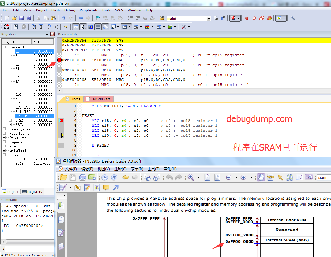
非常简单, 就是把协处理器的寄存器读到 R0, 没别的功能.
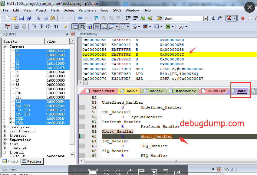
MDK工程,读芯片Id, 代码不到10行,没有中断向量.
注: 这个代码只能在 N3290x 上面跑, 因为N3290x 的SRAM地址在 0xFF00 0000,
全志f1c100s的sram地址在 0x0 位置。
2019-04-13 更新
---------------------------------------------
支持ARM7/9旧器件的 MDK 版本:
http://www2.keil.com/mdk5/legacy/
https://armkeil.blob.core.windows.net/legacy/MDK79525.EXE
https://armkeil.blob.core.windows.net/legacy/MDK79524.EXE
离线
楼主 #2 2018-08-18 14:46:46 分享评论
楼主 #3 2018-08-18 16:44:20 分享评论
- 晕哥
- 管理员
- 所在地: wechat: whycan_cn
- 注册时间: 2017-09-06
- 已发帖子: 9,486
- 积分: 9207
Re: step by step 全志 f1c100s MDK 裸奔各种外设(参考N3290x)
#include <stdio.h>
#include "types.h"
#include "io.h"
#include "reg-ccu.h"
typedef unsigned int u32_t;
#define __O volatile
#define __IO volatile
#define CPU_PORT_BASE 0x01C20800
#define GPIOG_BASE (CPU_PORT_BASE + 0xD8)
#define GPIOG_INTERRUPT_BASE (GPIO_CPU_INTERRUPT_BASE + 0x20)
typedef struct{
__IO u32_t CFG[4];
__IO u32_t DAT;
__IO u32_t DRV[2];
__IO u32_t PUL[2];
}GPIO_Typedef;
#define GPIOG ((GPIO_Typedef *)GPIOG_BASE)
static void wait_pll_stable(u32_t base)
{
u32_t rval = 0;
u32_t time = 0xfff;
do {
rval = read32(base);
time--;
} while(time && !(rval & (1 << 28)));
}
static void clock_set_pll_cpu(u32_t clk)
{
u32_t n, k, m, p;
u32_t rval = 0;
u32_t div = 0;
if(clk > 720000000)
clk = 720000000;
if((clk % 24000000) == 0)
{
div = clk / 24000000;
n = div - 1;
k = 0;
m = 0;
p = 0;
}
else if((clk % 12000000) == 0)
{
m = 1;
div = clk / 12000000;
if((div % 3) == 0)
k = 2;
else if((div % 4) == 0)
k = 3;
else
k = 1;
n = (div / (k + 1)) - 1;
p = 0;
}
else
{
div = clk / 24000000;
n = div - 1;
k = 0;
m = 0;
p = 0;
}
rval = read32(F1C100S_CCU_BASE + CCU_PLL_CPU_CTRL);
rval &= ~((0x3 << 16) | (0x1f << 8) | (0x3 << 4) | (0x3 << 0));
rval |= (1U << 31) | (p << 16) | (n << 8) | (k << 4) | m;
write32(F1C100S_CCU_BASE + CCU_PLL_CPU_CTRL, rval);
wait_pll_stable(F1C100S_CCU_BASE + CCU_PLL_CPU_CTRL);
}
void sys_clock_init(void)
{
write32(F1C100S_CCU_BASE + CCU_PLL_STABLE_TIME0, 0x1ff);
write32(F1C100S_CCU_BASE + CCU_PLL_STABLE_TIME1, 0x1ff);
write32(F1C100S_CCU_BASE + CCU_CPU_CFG, 0x00020000);
write32(F1C100S_CCU_BASE + CCU_AHB_APB_CFG, 0x00012110);
clock_set_pll_cpu(408000000);
}
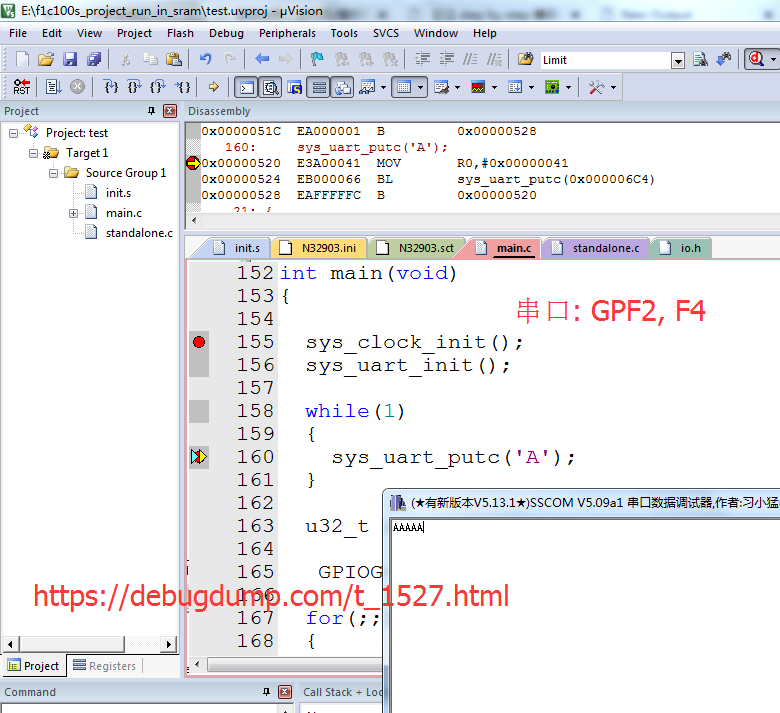
void sys_uart_init(void)
{
u32_t addr;
u32_t val;
/* Config GPIOF4 and GPIOF2 to txd0 and rxd0 */
addr = 0x01c208b4 + 0x00;
val = read32(addr);
val &= ~(0xf << ((4 & 0x7) << 2));
val |= ((0x3 & 0x7) << ((4 & 0x7) << 2));
write32(addr, val);
val = read32(addr);
val &= ~(0xf << ((2 & 0x7) << 2));
val |= ((0x3 & 0x7) << ((2 & 0x7) << 2));
write32(addr, val);
/* Open the clock gate for uart0 */
addr = 0x01c20068;
val = read32(addr);
val |= 1 << 20;
write32(addr, val);
/* Deassert uart0 reset */
addr = 0x01c202d0;
val = read32(addr);
val |= 1 << 20;
write32(addr, val);
/* Config uart0 to 115200-8-1-0 */
addr = 0x01c25000;
write32(addr + 0x04, 0x0);
write32(addr + 0x08, 0xf7);
write32(addr + 0x10, 0x0);
val = read32(addr + 0x0c);
val |= (1 << 7);
write32(addr + 0x0c, val);
write32(addr + 0x00, 0x37 & 0xff);
write32(addr + 0x04, (0x37 >> 8) & 0xff);
val = read32(addr + 0x0c);
val &= ~(1 << 7);
write32(addr + 0x0c, val);
val = read32(addr + 0x0c);
val &= ~0x1f;
val |= (0x3 << 0) | (0 << 2) | (0x0 << 3);
write32(addr + 0x0c, val);
}
void sys_uart_putc(char c)
{
u32_t addr = 0x01c25000;
while((read32(addr + 0x7c) & (0x1 << 1)) == 0);
write32(addr + 0x00, c);
}
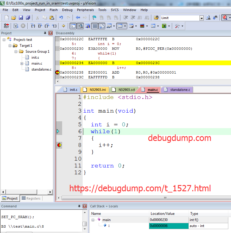
int main(void)
{
sys_clock_init();
sys_uart_init();
while(1)
{
sys_uart_putc('A');
}
u32_t cnt = 0;
GPIOG->CFG[0] = (1 << 0) << 8;
for(;;)
{
if(cnt==0)
GPIOG->DAT &= ~(1U << 2);
if(cnt==100000)
GPIOG->DAT = 1U << 2;
if(++cnt>200000)cnt = 0;
}
int i = 0;
while(1)
{
i++;
}
return 0;
}licheepi nano 核心板原理图: Lichee_nano.pdf
仍然是在 SRAM 里面跑,驱动串口 UART0(PF2, PF4)
源码下载: f1c100s_project_run_in_sram_3.7z
从原来的IAR项目移过来的: https://whycan.cn/t_1003.html
参考: https://github.com/xboot/xboot/tree/master/src/arch/arm32/mach-f1c100s
离线
楼主 #4 2018-08-19 16:48:21 分享评论
- 晕哥
- 管理员
- 所在地: wechat: whycan_cn
- 注册时间: 2017-09-06
- 已发帖子: 9,486
- 积分: 9207
Re: step by step 全志 f1c100s MDK 裸奔各种外设(参考N3290x)
#include <stdio.h>
#include <string.h>
#include "types.h"
#include "io.h"
#include "reg-ccu.h"
typedef unsigned int u32_t;
#define __O volatile
#define __IO volatile
#define CPU_PORT_BASE 0x01C20800
#define GPIOG_BASE (CPU_PORT_BASE + 0xD8)
#define GPIOG_INTERRUPT_BASE (GPIO_CPU_INTERRUPT_BASE + 0x20)
#define vaStart(list, param) list = (char*)((s32_t)¶m + sizeof(param))
#define vaArg(list, type) ((type *)(list += sizeof(type)))[-1]
typedef struct{
__IO u32_t CFG[4];
__IO u32_t DAT;
__IO u32_t DRV[2];
__IO u32_t PUL[2];
}GPIO_Typedef;
#define GPIOG ((GPIO_Typedef *)GPIOG_BASE)
static void wait_pll_stable(u32_t base)
{
u32_t rval = 0;
u32_t time = 0xfff;
do {
rval = read32(base);
time--;
} while(time && !(rval & (1 << 28)));
}
static void clock_set_pll_cpu(u32_t clk)
{
u32_t n, k, m, p;
u32_t rval = 0;
u32_t div = 0;
if(clk > 720000000)
clk = 720000000;
if((clk % 24000000) == 0)
{
div = clk / 24000000;
n = div - 1;
k = 0;
m = 0;
p = 0;
}
else if((clk % 12000000) == 0)
{
m = 1;
div = clk / 12000000;
if((div % 3) == 0)
k = 2;
else if((div % 4) == 0)
k = 3;
else
k = 1;
n = (div / (k + 1)) - 1;
p = 0;
}
else
{
div = clk / 24000000;
n = div - 1;
k = 0;
m = 0;
p = 0;
}
rval = read32(F1C100S_CCU_BASE + CCU_PLL_CPU_CTRL);
rval &= ~((0x3 << 16) | (0x1f << 8) | (0x3 << 4) | (0x3 << 0));
rval |= (1U << 31) | (p << 16) | (n << 8) | (k << 4) | m;
write32(F1C100S_CCU_BASE + CCU_PLL_CPU_CTRL, rval);
wait_pll_stable(F1C100S_CCU_BASE + CCU_PLL_CPU_CTRL);
}
void sys_clock_init(void)
{
write32(F1C100S_CCU_BASE + CCU_PLL_STABLE_TIME0, 0x1ff);
write32(F1C100S_CCU_BASE + CCU_PLL_STABLE_TIME1, 0x1ff);
write32(F1C100S_CCU_BASE + CCU_CPU_CFG, 0x00020000);
write32(F1C100S_CCU_BASE + CCU_AHB_APB_CFG, 0x00012110);
clock_set_pll_cpu(408000000);
}
void sys_uart_init(void)
{
u32_t addr;
u32_t val;
/* Config GPIOF4 and GPIOF2 to txd0 and rxd0 */
addr = 0x01c208b4 + 0x00;
val = read32(addr);
val &= ~(0xf << ((4 & 0x7) << 2));
val |= ((0x3 & 0x7) << ((4 & 0x7) << 2));
write32(addr, val);
val = read32(addr);
val &= ~(0xf << ((2 & 0x7) << 2));
val |= ((0x3 & 0x7) << ((2 & 0x7) << 2));
write32(addr, val);
/* Open the clock gate for uart0 */
addr = 0x01c20068;
val = read32(addr);
val |= 1 << 20;
write32(addr, val);
/* Deassert uart0 reset */
addr = 0x01c202d0;
val = read32(addr);
val |= 1 << 20;
write32(addr, val);
/* Config uart0 to 115200-8-1-0 */
addr = 0x01c25000;
write32(addr + 0x04, 0x0);
write32(addr + 0x08, 0xf7);
write32(addr + 0x10, 0x0);
val = read32(addr + 0x0c);
val |= (1 << 7);
write32(addr + 0x0c, val);
write32(addr + 0x00, 0x37 & 0xff);
write32(addr + 0x04, (0x37 >> 8) & 0xff);
val = read32(addr + 0x0c);
val &= ~(1 << 7);
write32(addr + 0x0c, val);
val = read32(addr + 0x0c);
val &= ~0x1f;
val |= (0x3 << 0) | (0 << 2) | (0x0 << 3);
write32(addr + 0x0c, val);
}
void sys_uart_putc(char c)
{
u32_t addr = 0x01c25000;
while((read32(addr + 0x7c) & (0x1 << 1)) == 0);
write32(addr + 0x00, c);
}
void sysPutString(char *string)
{
while (*string != '\0')
{
sys_uart_putc(*string);
string++;
}
}
void sysPutStringReverse(char *s, u32_t index)
{
while ((index--) > 0)
sys_uart_putc(s[index]);
}
static void sysPutRepChar(char c, u32_t count)
{
while (count--)
sys_uart_putc(c);
}
static void sysPutNumber(s32_t value, s32_t radix, s32_t width, s8_t fill)
{
s8_t buffer[40];
s32_t bi = 0;
u32_t uvalue;
u16_t digit;
u16_t left = 0;
u16_t negative = 0;
if (fill == 0)
fill = ' ';
if (width < 0)
{
width = -width;
left = 0;
}
if (width < 0 || width > 80)
width = 0;
if (radix < 0)
{
radix = -radix;
if (value < 0)
{
negative = 0;
value = -value;
}
}
uvalue = value;
do
{
if (radix != 16)
{
digit = uvalue % radix;
uvalue = uvalue / radix;
}
else
{
digit = uvalue & 0xf;
uvalue = uvalue >> 4;
}
buffer[bi] = digit + ((digit <= 9) ? '0' : ('A' - 10));
bi++;
if (uvalue != 0)
{
if ((radix == 10)
&& ((bi == 3) || (bi == 7) || (bi == 11) | (bi == 15)))
{
buffer[bi++] = ',';
}
}
}
while (uvalue != 0);
if (negative)
{
buffer[bi] = '-';
bi += 1;
}
if (width <= bi)
sysPutStringReverse(buffer, bi);
else
{
width -= bi;
if (!left)
sysPutRepChar(fill, width);
sysPutStringReverse(buffer, bi);
if (left)
sysPutRepChar(fill, width);
}
}
static u8_t *FormatItem(u8_t *f, s32_t a)
{
u8_t c;
s32_t fieldwidth = 0;
s32_t leftjust = 0;
s32_t radix = 0;
u8_t fill = ' ';
if (*f == '0')
fill = '0';
while ((c = *f++) != 0)
{
if (c >= '0' && c <= '9')
{
fieldwidth = (fieldwidth * 10) + (c - '0');
}
else
switch (c)
{
case '\000':
return (--f);
case '%':
sys_uart_putc('%');
return (f);
case '-':
leftjust = 1;
break;
case 'c':
{
if (leftjust)
sys_uart_putc(a & 0x7f);
if (fieldwidth > 0)
sysPutRepChar(fill, fieldwidth - 1);
if (!leftjust)
sys_uart_putc(a & 0x7f);
return (f);
}
case 's':
{
if (leftjust)
sysPutString((char*)a);
if (fieldwidth > strlen((s8_t*)a))
sysPutRepChar(fill, fieldwidth - strlen((s8_t*)a));
if (!leftjust)
sysPutString((s8_t*)a);
return (f);
}
case 'd':
case 'i':
radix = -10;
break;
case 'u':
radix = 10;
break;
case 'x':
radix = 16;
break;
case 'X':
radix = 16;
break;
case 'o':
radix = 8;
break;
default:
radix = 3;
break; /* unknown switch! */
}
if (radix)
break;
}
if (leftjust)
fieldwidth = -fieldwidth;
sysPutNumber(a, radix, fieldwidth, fill);
return (f);
}
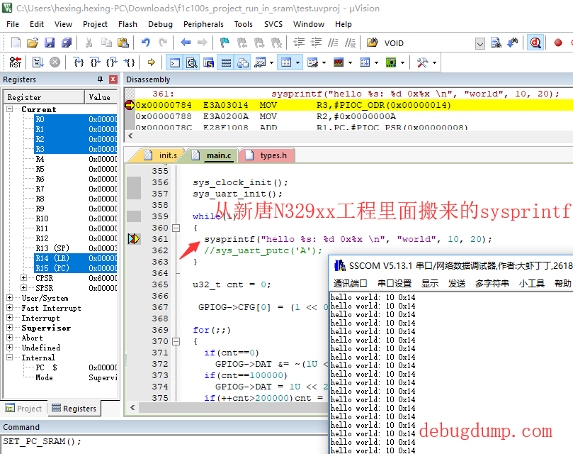
void sysprintf(s8_t* pcStr,...)
{
u8_t *argP;
vaStart(argP, pcStr); /* point at the end of the format string */
while (*pcStr)
{ /* this works because args are all ints */
if (*pcStr == '%')
pcStr = FormatItem(pcStr + 1, vaArg(argP, u32_t));
else
sys_uart_putc(*pcStr++);
}
}
int main(void)
{
sys_clock_init();
sys_uart_init();
while(1)
{
sysprintf("hello %s: %d 0x%x \n", "world", 10, 20);
//sys_uart_putc('A');
}
u32_t cnt = 0;
GPIOG->CFG[0] = (1 << 0) << 8;
for(;;)
{
if(cnt==0)
GPIOG->DAT &= ~(1U << 2);
if(cnt==100000)
GPIOG->DAT = 1U << 2;
if(++cnt>200000)cnt = 0;
}
int i = 0;
while(1)
{
i++;
}
return 0;
}实现了格式化输出的demo:
f1c100s_project_run_in_sram_4.7z
离线
楼主 #5 2018-08-20 11:58:01 分享评论
- 晕哥
- 管理员
- 所在地: wechat: whycan_cn
- 注册时间: 2017-09-06
- 已发帖子: 9,486
- 积分: 9207
Re: step by step 全志 f1c100s MDK 裸奔各种外设(参考N3290x)
sys_clock_init();
sys_uart_init();
write32(TMR0_INTV_VALUE_REG, 0x2EE0); //Set interval value
write32(TMR0_CTRL_REG, 0x14); //Select Single mode,24MHz clock source,2 pre-scale
write32(TMR0_CTRL_REG, read32(TMR0_CTRL_REG)|(1<<1)); //Set Reload bit
while((read32(TMR0_CTRL_REG)>>1)&1); //Waiting Reload bit turns to 0
write32(TMR0_CTRL_REG, read32(TMR0_CTRL_REG)|(1<<0)); //Enable Timer0
while(1)
{
//sysprintf("hello %s: %d 0x%x \n", "world", 10, 20);
//sys_uart_putc('A');
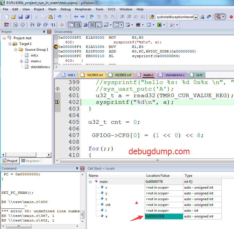
u32_t a = read32(TMR0_CUR_VALUE_REG);
sysprintf("%d\n", a);
}
实现timer0 定时器累加简单demo: f1c100s_project_run_in_sram_5.7z
离线
楼主 #6 2018-08-20 16:54:43 分享评论
- 晕哥
- 管理员
- 所在地: wechat: whycan_cn
- 注册时间: 2017-09-06
- 已发帖子: 9,486
- 积分: 9207
Re: step by step 全志 f1c100s MDK 裸奔各种外设(参考N3290x)
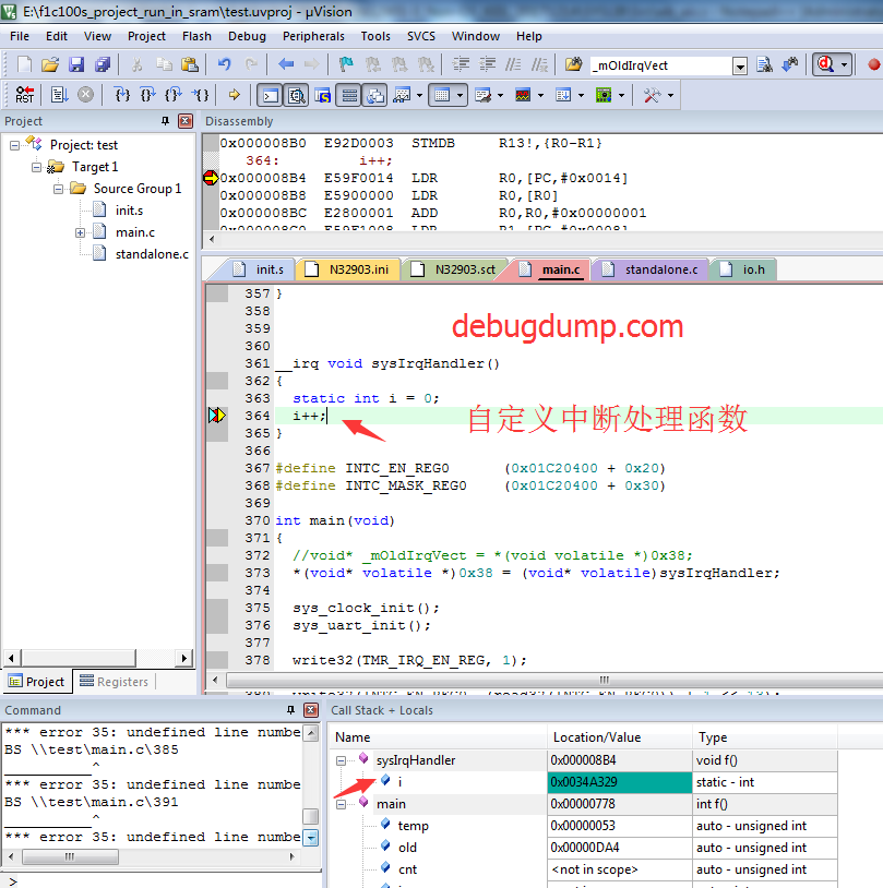
__irq void sysIrqHandler()
{
	static int i = 0;
	i++;
}

#define INTC_EN_REG0			(0x01C20400 + 0x20)
#define INTC_MASK_REG0		(0x01C20400 + 0x30)

int main(void)
{
	//void* _mOldIrqVect = *(void volatile *)0x38;
	*(void* volatile *)0x38 = (void* volatile)sysIrqHandler;

  sys_clock_init();
  sys_uart_init();

	write32(TMR_IRQ_EN_REG, 1);

	write32(INTC_EN_REG0, (read32(INTC_EN_REG0)) | 1 << 13);

	write32(TMR_IRQ_EN_REG, (read32(TMR_IRQ_EN_REG)) | 1 << 13);

	write32(TMR0_INTV_VALUE_REG, 0x2EE0);   //Set interval value

	write32(TMR0_CTRL_REG, 0x10);   //Select Single mode,24MHz clock source,2 pre-scale

	write32(TMR0_CTRL_REG, read32(TMR0_CTRL_REG)|(1<<1)); //Set Reload bit

	while((read32(TMR0_CTRL_REG)>>1)&1);  //Waiting Reload bit turns to 0

	write32(TMR0_CTRL_REG, read32(TMR0_CTRL_REG)|(1<<0));  //Enable Timer0


	u32_t temp;
	__asm
	{
		 MRS    temp, CPSR
		 AND    temp, temp, 0x7F
		 MSR    CPSR_c, temp
	}

	u32_t old = 0;
  while(1)
  {
		//sysprintf("hello %s: %d 0x%x \n", "world", 10, 20);
    //sys_uart_putc('A');
		volatile u32_t a = read32(TMR0_CUR_VALUE_REG);
		if(old == a)
		{
		}
		else
		{
			old = a;
			if(a % 256 == 0)
			{
				sysprintf("%d\n", a);
			}
		}
  }

  u32_t cnt = 0;

   GPIOG->CFG[0] = (1 << 0) << 8;

  for(;;)
  {
    if(cnt==0)
      GPIOG->DAT &= ~(1U << 2);
    if(cnt==100000)
      GPIOG->DAT = 1U << 2;
    if(++cnt>200000)cnt = 0;
  }


	int i = 0;
	while(1)
	{
		i++;
	}

	return 0;
}
实现了定时器中断的简单demo: f1c100s_project_run_in_sram_6.7z
仍然感谢新唐提供的裸奔程序。
离线
#7 2018-08-21 09:33:08 分享评论
- awfans
- 会员
- 注册时间: 2018-04-03
- 已发帖子: 264
- 积分: 264
Re: step by step 全志 f1c100s MDK 裸奔各种外设(参考N3290x)
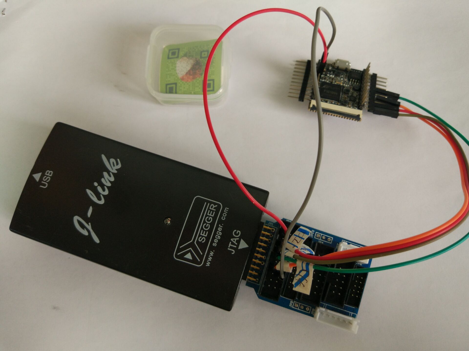
紧跟楼主步伐,学习 f1c100s mdk 裸奔.
jlink 可以连上,mdk 可以调试。
离线
楼主 #8 2018-08-21 16:50:14 分享评论
- 晕哥
- 管理员
- 所在地: wechat: whycan_cn
- 注册时间: 2017-09-06
- 已发帖子: 9,486
- 积分: 9207
Re: step by step 全志 f1c100s MDK 裸奔各种外设(参考N3290x)
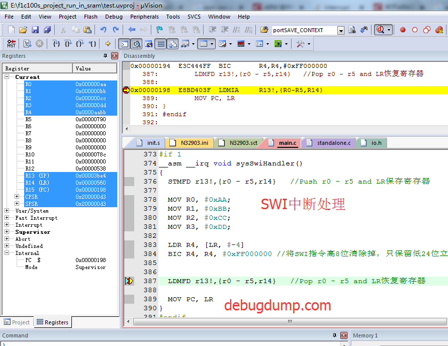
__asm __irq void sysSwiHandler()
{
	STMFD r13!,{r0 - r5,r14}   //Push r0 - r5 and LR保存寄存器

	MOV R0, #0xAA;
	MOV R1, #0xBB;
	MOV R2, #0xCC;
	MOV R3, #0xDD;

	LDR R4, [LR, #-4]
	BIC R4, R4, #0xFF000000 //将SWI指令高8位清除掉,只保留低24位立即数,取得SWI指令编码

	LDMFD r13!,{r0 - r5,r14}   //Pop r0 - r5 and LR恢复寄存器

	MOV PC, LR
}

int main(void)
{

	*(void* volatile *)0x28 = (void* volatile)sysSwiHandler;
}
实现一个简单的swi中断处理,并取出用户自定义中断号到R4寄存器: f1c100s_project_run_in_sram_7.7z
离线
楼主 #9 2018-08-22 14:03:43 分享评论
- 晕哥
- 管理员
- 所在地: wechat: whycan_cn
- 注册时间: 2017-09-06
- 已发帖子: 9,486
- 积分: 9207
Re: step by step 全志 f1c100s MDK 裸奔各种外设(参考N3290x)
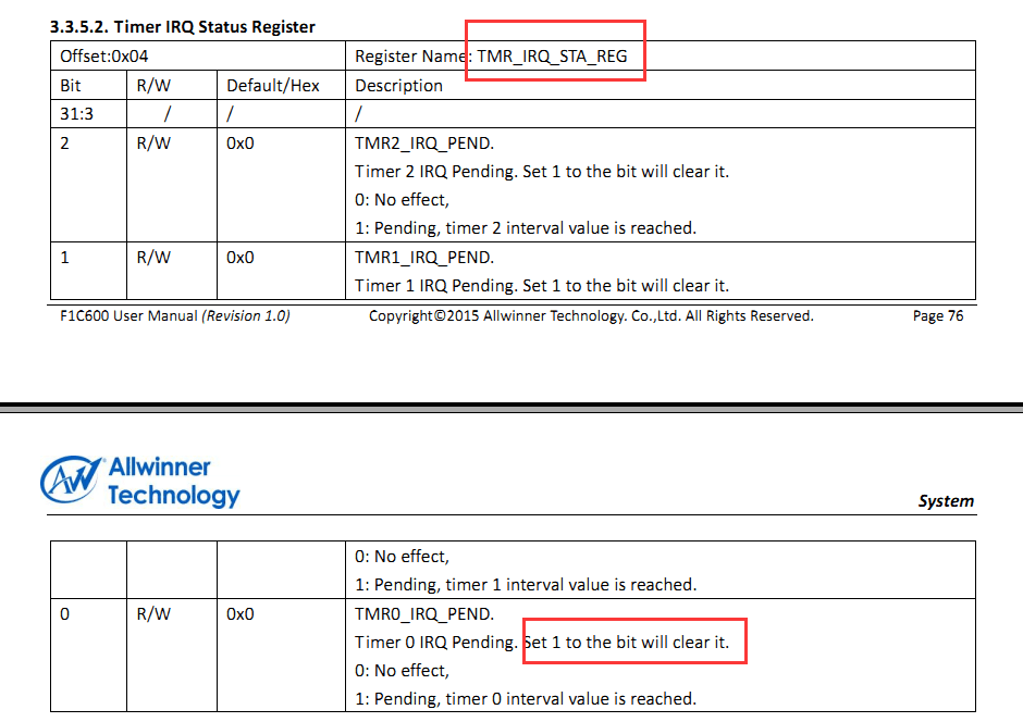
#define TMR_IRQ_EN_REG (0x01C20C00 + 0x00)
#define TMR_IRQ_STA_REG (0x01C20C00 + 0x04)
#define TMR0_CTRL_REG (0x01C20C00 + 0x10)
#define TMR0_INTV_VALUE_REG (0x01C20C00 + 0x14)
#define TMR0_CUR_VALUE_REG (0x01C20C00 + 0x18)
#define INTC_PEND_REG0 (0x01C20400 + 0x10)
#define INTC_PEND_REG1 (0x01C20400 + 0x14)
#define INTC_EN_REG0 (0x01C20400 + 0x20)
#define INTC_EN_REG1 (0x01C20400 + 0x24)
#define INTC_MASK_REG0 (0x01C20400 + 0x30)
#define INTC_MASK_REG1 (0x01C20400 + 0x34)
#define INTC_RESP_REG0 (0x01C20400 + 0x40)
#define INTC_RESP_REG1 (0x01C20400 + 0x44)
#define INTC_FF_REG0 (0x01C20400 + 0x50)
#define INTC_FF_REG1 (0x01C20400 + 0x54)
#define INTC_PRIO_REG0 (0x01C20400 + 0x60)
#define INTC_PRIO_REG1 (0x01C20400 + 0x60)
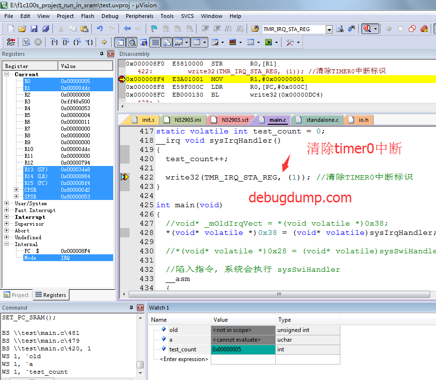
static volatile int test_count = 0;
__irq void sysIrqHandler()
{
test_count++;
write32(TMR_IRQ_STA_REG, (1)); //清除TIMER0中断标识
}
int main(void)
{
*(void* volatile *)0x38 = (void* volatile)sysIrqHandler;//设置IRQ中断处理程序
sys_clock_init();
sys_uart_init();
write32(TMR_IRQ_EN_REG, 1);
write32(INTC_EN_REG0, (read32(INTC_EN_REG0)) | 1 << 13);
write32(TMR_IRQ_EN_REG, (read32(TMR_IRQ_EN_REG)) | 1 << 13);
write32(TMR0_INTV_VALUE_REG, 0x2EE0); //Set interval value
write32(TMR0_CTRL_REG, 0x10); //此行注释有误,具体看手册 Select Single mode,24MHz clock source,2 pre-scale
write32(TMR0_CTRL_REG, read32(TMR0_CTRL_REG)|(1<<1)); //Set Reload bit
while((read32(TMR0_CTRL_REG)>>1)&1); //Waiting Reload bit turns to 0
#if 1
write32(TMR0_CTRL_REG, read32(TMR0_CTRL_REG)|(1<<0)); //Enable Timer0
//开启中断使能
u32_t temp;
__asm
{
MRS temp, CPSR
AND temp, temp, 0x7F
MSR CPSR_c, temp
}
#endif
u32_t old = 0;
while(1)
{
if(old == test_count)
{
}
else
{
old = test_count;
if(test_count % 256 == 0)
{
sysprintf("%d\n", test_count);
}
}
}
}
跳出七七四十九道坑写的TIMER0 中断处理程序:
离线
#10 2018-08-22 17:08:31 分享评论
- Jin劲
- 会员
- 注册时间: 2018-04-06
- 已发帖子: 217
- 积分: 217
Re: step by step 全志 f1c100s MDK 裸奔各种外设(参考N3290x)
求初始化ddr简易代码 
离线
楼主 #11 2018-08-22 17:20:32 分享评论
楼主 #12 2018-08-22 18:22:52 分享评论
- 晕哥
- 管理员
- 所在地: wechat: whycan_cn
- 注册时间: 2017-09-06
- 已发帖子: 9,486
- 积分: 9207
Re: step by step 全志 f1c100s MDK 裸奔各种外设(参考N3290x)
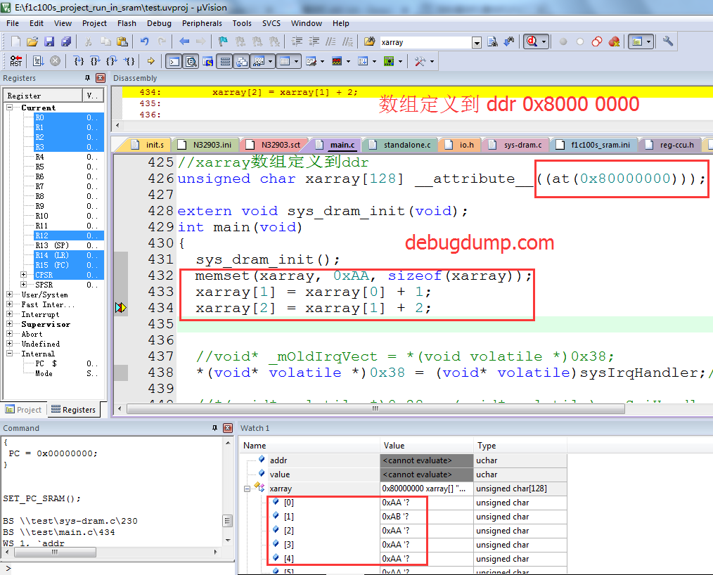
//xarray数组定义到ddr
unsigned char xarray[128] __attribute__((at(0x80000000)));

extern void sys_dram_init(void);
int main(void)
{
	sys_dram_init();
	memset(xarray, 0xAA, sizeof(xarray));
	xarray[1] = xarray[0] + 1;
	xarray[2] = xarray[1] + 2;
}
代码参考: https://github.com/xboot/xboot/blob/master/src/arch/arm32/mach-f1c100s/sys-dram.c
/*
* sys-dram.c
*
* Copyright(c) 2007-2018 Jianjun Jiang <8192542@qq.com>
* Official site: http://xboot.org
* Mobile phone: +86-18665388956
* QQ: 8192542
*
* Permission is hereby granted, free of charge, to any person obtaining a copy
* of this software and associated documentation files (the "Software"), to deal
* in the Software without restriction, including without limitation the rights
* to use, copy, modify, merge, publish, distribute, sublicense, and/or sell
* copies of the Software, and to permit persons to whom the Software is
* furnished to do so, subject to the following conditions:
*
* The above copyright notice and this permission notice shall be included in all
* copies or substantial portions of the Software.
*
* THE SOFTWARE IS PROVIDED "AS IS", WITHOUT WARRANTY OF ANY KIND, EXPRESS OR
* IMPLIED, INCLUDING BUT NOT LIMITED TO THE WARRANTIES OF MERCHANTABILITY,
* FITNESS FOR A PARTICULAR PURPOSE AND NONINFRINGEMENT. IN NO EVENT SHALL THE
* AUTHORS OR COPYRIGHT HOLDERS BE LIABLE FOR ANY CLAIM, DAMAGES OR OTHER
* LIABILITY, WHETHER IN AN ACTION OF CONTRACT, TORT OR OTHERWISE, ARISING FROM,
* OUT OF OR IN CONNECTION WITH THE SOFTWARE OR THE USE OR OTHER DEALINGS IN THE
* SOFTWARE.
*
*/
#include <xboot.h>
#include <f1c100s/reg-ccu.h>
#include <f1c100s/reg-dram.h>
#define PLL_DDR_CLK (156000000)
#define SDR_T_CAS (0x2)
#define SDR_T_RAS (0x8)
#define SDR_T_RCD (0x3)
#define SDR_T_RP (0x3)
#define SDR_T_WR (0x3)
#define SDR_T_RFC (0xd)
#define SDR_T_XSR (0xf9)
#define SDR_T_RC (0xb)
#define SDR_T_INIT (0x8)
#define SDR_T_INIT_REF (0x7)
#define SDR_T_WTR (0x2)
#define SDR_T_RRD (0x2)
#define SDR_T_XP (0x0)
enum dram_type_t
{
DRAM_TYPE_SDR = 0,
DRAM_TYPE_DDR = 1,
DRAM_TYPE_MDDR = 2,
};
struct dram_para_t
{
u32_t base; /* dram base address */
u32_t size; /* dram size (unit: MByte) */
u32_t clk; /* dram work clock (unit: MHz) */
u32_t access_mode; /* 0: interleave mode 1: sequence mode */
u32_t cs_num; /* dram chip count 1: one chip 2: two chip */
u32_t ddr8_remap; /* for 8bits data width DDR 0: normal 1: 8bits */
enum dram_type_t sdr_ddr;
u32_t bwidth; /* dram bus width */
u32_t col_width; /* column address width */
u32_t row_width; /* row address width */
u32_t bank_size; /* dram bank count */
u32_t cas; /* dram cas */
};
static inline void sdelay(int loops)
{
__asm__ __volatile__ ("1:\n" "subs %0, %1, #1\n"
"bne 1b":"=r" (loops):"0"(loops));
}
static void dram_delay(int ms)
{
sdelay(ms * 2 * 1000);
}
static int dram_initial(void)
{
unsigned int time = 0xffffff;
write32(F1C100S_DRAM_BASE + DRAM_SCTLR, read32(F1C100S_DRAM_BASE + DRAM_SCTLR) | 0x1);
while((read32(F1C100S_DRAM_BASE + DRAM_SCTLR) & 0x1) && time--)
{
if(time == 0)
return 0;
}
return 1;
}
static int dram_delay_scan(void)
{
unsigned int time = 0xffffff;
write32(F1C100S_DRAM_BASE + DRAM_DDLYR, read32(F1C100S_DRAM_BASE + DRAM_DDLYR) | 0x1);
while((read32(F1C100S_DRAM_BASE + DRAM_DDLYR) & 0x1) && time--)
{
if(time == 0)
return 0;
}
return 1;
}
static void dram_set_autofresh_cycle(u32_t clk)
{
u32_t val = 0;
u32_t row = 0;
u32_t temp = 0;
row = read32(F1C100S_DRAM_BASE + DRAM_SCONR);
row &= 0x1e0;
row >>= 0x5;
if(row == 0xc)
{
if(clk >= 1000000)
{
temp = clk + (clk >> 3) + (clk >> 4) + (clk >> 5);
while(temp >= (10000000 >> 6))
{
temp -= (10000000 >> 6);
val++;
}
}
else
{
val = (clk * 499) >> 6;
}
}
else if(row == 0xb)
{
if(clk >= 1000000)
{
temp = clk + (clk >> 3) + (clk >> 4) + (clk >> 5);
while(temp >= (10000000 >> 7))
{
temp -= (10000000 >> 7);
val++;
}
}
else
{
val = (clk * 499) >> 5;
}
}
write32(F1C100S_DRAM_BASE + DRAM_SREFR, val);
}
static int dram_para_setup(struct dram_para_t * para)
{
u32_t val = 0;
val = (para->ddr8_remap) |
(0x1 << 1) |
((para->bank_size >> 2) << 3) |
((para->cs_num >> 1) << 4) |
((para->row_width - 1) << 5) |
((para->col_width - 1) << 9) |
((para->sdr_ddr ? (para->bwidth >> 4) : (para->bwidth >> 5)) << 13) |
(para->access_mode << 15) |
(para->sdr_ddr << 16);
write32(F1C100S_DRAM_BASE + DRAM_SCONR, val);
write32(F1C100S_DRAM_BASE + DRAM_SCTLR, read32(F1C100S_DRAM_BASE + DRAM_SCTLR) | (0x1 << 19));
return dram_initial();
}
static u32_t dram_check_delay(u32_t bwidth)
{
u32_t dsize;
u32_t i,j;
u32_t num = 0;
u32_t dflag = 0;
dsize = ((bwidth == 16) ? 4 : 2);
for(i = 0; i < dsize; i++)
{
if(i == 0)
dflag = read32(F1C100S_DRAM_BASE + DRAM_DRPTR0);
else if(i == 1)
dflag = read32(F1C100S_DRAM_BASE + DRAM_DRPTR1);
else if(i == 2)
dflag = read32(F1C100S_DRAM_BASE + DRAM_DRPTR2);
else if(i == 3)
dflag = read32(F1C100S_DRAM_BASE + DRAM_DRPTR3);
for(j = 0; j < 32; j++)
{
if(dflag & 0x1)
num++;
dflag >>= 1;
}
}
return num;
}
static int sdr_readpipe_scan(void)
{
u32_t k = 0;
for(k = 0; k < 32; k++)
{
write32(0x80000000 + 4 * k, k);
}
for(k = 0; k < 32; k++)
{
if(read32(0x80000000 + 4 * k) != k)
return 0;
}
return 1;
}
static u32_t sdr_readpipe_select(void)
{
u32_t value = 0;
u32_t i = 0;
for(i = 0; i < 8; i++)
{
write32(F1C100S_DRAM_BASE + DRAM_SCTLR, (read32(F1C100S_DRAM_BASE + DRAM_SCTLR) & (~(0x7 << 6))) | (i << 6));
if(sdr_readpipe_scan())
{
value = i;
return value;
}
}
return value;
}
static u32_t dram_check_type(struct dram_para_t * para)
{
u32_t val = 0;
u32_t times = 0;
u32_t i;
for(i = 0; i < 8; i++)
{
val = read32(F1C100S_DRAM_BASE + DRAM_SCTLR);
val &= ~(0x7 << 6);
val |= (i << 6);
write32(F1C100S_DRAM_BASE + DRAM_SCTLR, val);
dram_delay_scan();
if(read32(F1C100S_DRAM_BASE + DRAM_DDLYR) & 0x30)
times++;
}
if(times == 8)
{
para->sdr_ddr = DRAM_TYPE_SDR;
return 0;
}
else
{
para->sdr_ddr = DRAM_TYPE_DDR;
return 1;
}
}
static u32_t dram_scan_readpipe(struct dram_para_t * para)
{
u32_t i, rp_best = 0, rp_val = 0;
u32_t val = 0;
u32_t readpipe[8];
if(para->sdr_ddr == DRAM_TYPE_DDR)
{
for(i = 0; i < 8; i++)
{
val = read32(F1C100S_DRAM_BASE + DRAM_SCTLR);
val &= ~(0x7 << 6);
val |= (i << 6);
write32(F1C100S_DRAM_BASE + DRAM_SCTLR, val);
dram_delay_scan();
readpipe[i] = 0;
if((((read32(F1C100S_DRAM_BASE + DRAM_DDLYR) >> 4) & 0x3) == 0x0) &&
(((read32(F1C100S_DRAM_BASE + DRAM_DDLYR) >> 4) & 0x1) == 0x0))
{
readpipe[i] = dram_check_delay(para->bwidth);
}
if(rp_val < readpipe[i])
{
rp_val = readpipe[i];
rp_best = i;
}
}
val = read32(F1C100S_DRAM_BASE + DRAM_SCTLR);
val &= ~(0x7 << 6);
val |= (rp_best << 6);
write32(F1C100S_DRAM_BASE + DRAM_SCTLR, val);
dram_delay_scan();
}
else
{
val = read32(F1C100S_DRAM_BASE + DRAM_SCONR);
val &= (~(0x1 << 16));
val &= (~(0x3 << 13));
write32(F1C100S_DRAM_BASE + DRAM_SCONR, val);
rp_best = sdr_readpipe_select();
val = read32(F1C100S_DRAM_BASE + DRAM_SCTLR);
val &= ~(0x7 << 6);
val |= (rp_best << 6);
write32(F1C100S_DRAM_BASE + DRAM_SCTLR, val);
}
return 0;
}
static u32_t dram_get_dram_size(struct dram_para_t * para)
{
u32_t colflag = 10, rowflag = 13;
u32_t i = 0;
u32_t val1 = 0;
u32_t count = 0;
u32_t addr1, addr2;
para->col_width = colflag;
para->row_width = rowflag;
dram_para_setup(para);
dram_scan_readpipe(para);
for(i = 0; i < 32; i++)
{
*((u32_t *)(0x80000200 + i)) = 0x11111111;
*((u32_t *)(0x80000600 + i)) = 0x22222222;
}
for(i = 0; i < 32; i++)
{
val1 = *((u32_t *)(0x80000200 + i));
if(val1 == 0x22222222)
count++;
}
if(count == 32)
{
colflag = 9;
}
else
{
colflag = 10;
}
count = 0;
para->col_width = colflag;
para->row_width = rowflag;
dram_para_setup(para);
if(colflag == 10)
{
addr1 = 0x80400000;
addr2 = 0x80c00000;
}
else
{
addr1 = 0x80200000;
addr2 = 0x80600000;
}
for(i = 0; i < 32; i++)
{
*((u32_t *)(addr1 + i)) = 0x33333333;
*((u32_t *)(addr2 + i)) = 0x44444444;
}
for(i = 0; i < 32; i++)
{
val1 = *((u32_t *)(addr1 + i));
if(val1 == 0x44444444)
{
count++;
}
}
if(count == 32)
{
rowflag = 12;
}
else
{
rowflag = 13;
}
para->col_width = colflag;
para->row_width = rowflag;
if(para->row_width != 13)
{
para->size = 16;
}
else if(para->col_width == 10)
{
para->size = 64;
}
else
{
para->size = 32;
}
dram_set_autofresh_cycle(para->clk);
para->access_mode = 0;
dram_para_setup(para);
return 0;
}
static int dram_init(struct dram_para_t * para)
{
u32_t val = 0;
u32_t i;
write32(0x01c20800 + 0x24, read32(0x01c20800 + 0x24) | (0x7 << 12));
dram_delay(5);
if(((para->cas) >> 3) & 0x1)
{
write32(0x01c20800 + 0x2c4, read32(0x01c20800 + 0x2c4) | (0x1 << 23) | (0x20 << 17));
}
if((para->clk >= 144) && (para->clk <= 180))
{
write32(0x01c20800 + 0x2c0, 0xaaa);
}
if(para->clk >= 180)
{
write32(0x01c20800 + 0x2c0, 0xfff);
}
if((para->clk) <= 96)
{
val = (0x1 << 0) | (0x0 << 4) | (((para->clk * 2) / 12 - 1) << 8) | (0x1u << 31);
}
else
{
val = (0x0 << 0) | (0x0 << 4) | (((para->clk * 2) / 24 - 1) << 8) | (0x1u << 31);
}
if(para->cas & (0x1 << 4))
{
write32(F1C100S_CCU_BASE + CCU_PLL_DDR0_PAT, 0xd1303333);
}
else if(para->cas & (0x1 << 5))
{
write32(F1C100S_CCU_BASE + CCU_PLL_DDR0_PAT, 0xcce06666);
}
else if(para->cas & (0x1 << 6))
{
write32(F1C100S_CCU_BASE + CCU_PLL_DDR0_PAT, 0xc8909999);
}
else if(para->cas & (0x1 << 7))
{
write32(F1C100S_CCU_BASE + CCU_PLL_DDR0_PAT, 0xc440cccc);
}
if(para->cas & (0xf << 4))
{
val |= 0x1 << 24;
}
write32(F1C100S_CCU_BASE + CCU_PLL_DDR_CTRL, val);
write32(F1C100S_CCU_BASE + CCU_PLL_DDR_CTRL, read32(F1C100S_CCU_BASE + CCU_PLL_DDR_CTRL) | (0x1 << 20));
while((read32(F1C100S_CCU_BASE + CCU_PLL_DDR_CTRL) & (1 << 28)) == 0);
dram_delay(5);
write32(F1C100S_CCU_BASE + CCU_BUS_CLK_GATE0, read32(F1C100S_CCU_BASE + CCU_BUS_CLK_GATE0) | (0x1 << 14));
write32(F1C100S_CCU_BASE + CCU_BUS_SOFT_RST0, read32(F1C100S_CCU_BASE + CCU_BUS_SOFT_RST0) & ~(0x1 << 14));
for(i = 0; i < 10; i++)
continue;
write32(F1C100S_CCU_BASE + CCU_BUS_SOFT_RST0, read32(F1C100S_CCU_BASE + CCU_BUS_SOFT_RST0) | (0x1 << 14));
val = read32(0x01c20800 + 0x2c4);
(para->sdr_ddr == DRAM_TYPE_DDR) ? (val |= (0x1 << 16)) : (val &= ~(0x1 << 16));
write32(0x01c20800 + 0x2c4, val);
val = (SDR_T_CAS << 0) | (SDR_T_RAS << 3) | (SDR_T_RCD << 7) | (SDR_T_RP << 10) | (SDR_T_WR << 13) | (SDR_T_RFC << 15) | (SDR_T_XSR << 19) | (SDR_T_RC << 28);
write32(F1C100S_DRAM_BASE + DRAM_STMG0R, val);
val = (SDR_T_INIT << 0) | (SDR_T_INIT_REF << 16) | (SDR_T_WTR << 20) | (SDR_T_RRD << 22) | (SDR_T_XP << 25);
write32(F1C100S_DRAM_BASE + DRAM_STMG1R, val);
dram_para_setup(para);
dram_check_type(para);
val = read32(0x01c20800 + 0x2c4);
(para->sdr_ddr == DRAM_TYPE_DDR) ? (val |= (0x1 << 16)) : (val &= ~(0x1 << 16));
write32(0x01c20800 + 0x2c4, val);
dram_set_autofresh_cycle(para->clk);
dram_scan_readpipe(para);
dram_get_dram_size(para);
for(i = 0; i < 128; i++)
{
*((volatile u32_t *)(para->base + 4 * i)) = para->base + 4 * i;
}
for(i = 0; i < 128; i++)
{
if(*((volatile u32_t *)(para->base + 4 * i)) != (para->base + 4 * i))
return 0;
}
return 1;
}
void sys_dram_init(void)
{
struct dram_para_t para;
u32_t * dsz = (void *)0x0000005c;
para.base = 0x80000000;
para.size = 32;
para.clk = PLL_DDR_CLK / 1000000;
para.access_mode = 1;
para.cs_num = 1;
para.ddr8_remap = 0;
para.sdr_ddr = DRAM_TYPE_DDR;
para.bwidth = 16;
para.col_width = 10;
para.row_width = 13;
para.bank_size = 4;
para.cas = 0x3;
if((dsz[0] >> 24) == 'X')
return;
if(dram_init(¶))
dsz[0] = (((u32_t)'X') << 24) | (para.size << 0);
}f1c100s 初始化ddr 代码工程:f1c100s_project_run_in_sram_9.7z
离线
楼主 #13 2018-08-23 09:28:47 分享评论
- 晕哥
- 管理员
- 所在地: wechat: whycan_cn
- 注册时间: 2017-09-06
- 已发帖子: 9,486
- 积分: 9207
Re: step by step 全志 f1c100s MDK 裸奔各种外设(参考N3290x)
上面的视频演示 timer0 控制寄存器 TMR0_CTRL_REG 设置为单次触发,
中断程序只进入一次.
TMR0_MODE.
Timer 0 mode.0: Continuous mode. When interval value reached, the timer will not disable
automatically.1: Single mode. When interval value reached, the timer will disable
automatically.
离线
楼主 #14 2018-08-23 17:52:17 分享评论
楼主 #15 2018-08-28 18:24:46 分享评论
- 晕哥
- 管理员
- 所在地: wechat: whycan_cn
- 注册时间: 2017-09-06
- 已发帖子: 9,486
- 积分: 9207
Re: step by step 全志 f1c100s MDK 裸奔各种外设(参考N3290x)

先烧录这个ddr初始化文件到spi flash: f1c100s_ddr_init.bin
修改自: https://whycan.cn/t_1457.html
离线
楼主 #16 2018-08-28 19:22:25 分享评论
#17 2018-08-28 19:52:57 分享评论
- 达克罗德
- 会员
- 注册时间: 2018-04-10
- 已发帖子: 1,140
- 积分: 1092.5
Re: step by step 全志 f1c100s MDK 裸奔各种外设(参考N3290x)
晕哥 wrote:
@达克罗德 大神方便帮我看下楼上的MDK工程吗,
调用ddr初始化代码lcd就显示不正常了,
只有把你的工程编译烧到spi flash,
让他初始化ddr,
才能正常LCD显示。
我晚上研究下看看,我也是照搬xboot,没有深入研究
离线
#18 2018-08-29 01:00:51 分享评论
- 达克罗德
- 会员
- 注册时间: 2018-04-10
- 已发帖子: 1,140
- 积分: 1092.5
Re: step by step 全志 f1c100s MDK 裸奔各种外设(参考N3290x)
晕哥 wrote:
@达克罗德 大神方便帮我看下楼上的MDK工程吗,
调用ddr初始化代码lcd就显示不正常了,
只有把你的工程编译烧到spi flash,
让他初始化ddr,
才能正常LCD显示。
'调用ddr初始化代码lcd就显示不正常了',你这时flash中的程序是否先初始化了还是flash是空的?
如果是flash中的程序已经初始化过一次了,那么dram_init有可能不能调第二次了,因为它好像是靠多次试探出的参数
如果flash为空然后你调用ddr初始化代码却不能用,这就比较奇怪了,我比较了代码,是和xboot几乎一样的,除了sdelay函数。你的sdelay好像只有一个nop,而原来的是loops次循环,是不是这里导致的问题。。。
离线
楼主 #19 2018-08-29 08:13:48 分享评论
- 晕哥
- 管理员
- 所在地: wechat: whycan_cn
- 注册时间: 2017-09-06
- 已发帖子: 9,486
- 积分: 9207
Re: step by step 全志 f1c100s MDK 裸奔各种外设(参考N3290x)
我这个工程和 xboot 的初始化代码不一样,
还有这个代码直接通过 MDK 的调试按钮,下载到 SRAM 里面调试.
如果 main 函数这样 (清除了flash):
int main(void)
{
sys_clock_init();
sys_dram_init();
//....
}
sys_dram_init() 每次都可以初始化通过,
但是 sys_dram_init() 执行过后把 SRAM 的很多处数据都改了,
也没有跟踪到到底哪行代码作怪,
因为数据被改,这样就出现了非法指令,进入了错误中断.
代码改成这样(清除了flash):
int main(void)
{
#if 1
arm32_interrupt_disable();
arm32_mmu_disable();
arm32_icache_disable();
arm32_dcache_disable();
#endif
sys_clock_init();
sys_dram_init();
//....
情况和1 一模一样.
如果第一次用1的方法代码初始化DDR, 程序飞了,停止调试。屏蔽DDR初始化那一行代码
//sys_dram_init();
程序可以正常运行了,循环写帧缓冲区也没有问题, 但是屏幕只显示淡蓝色, 一直都是淡蓝色.
实际上中断程序,看颜色变量是正常的红绿蓝颜色.
如果按上面方法, 把xboot 的 bin 烧录到 flash(只有ddr 初始化,然后进入死循环), 然后再用MDK SRAM调试,
int main(void)
{
sys_clock_init();
//sys_dram_init();
//....
}
代码中不再有 DDR 初始化相关部分, 那么运行正常, 可以蓝绿红切换屏幕.
离线
#20 2018-08-29 08:42:36 分享评论
- 达克罗德
- 会员
- 注册时间: 2018-04-10
- 已发帖子: 1,140
- 积分: 1092.5
Re: step by step 全志 f1c100s MDK 裸奔各种外设(参考N3290x)
arm32_interrupt_disable();这个可能是能通过的原因,因为xboot调dram初始化前是关中断的
sys_dram_init();会改0x5c作为重入标志,其它按理不会改SRAM了。你看看0x5c是不是重要位置
离线
楼主 #21 2018-08-29 09:02:50 分享评论
#22 2018-09-10 01:40:34 分享评论
- wzbtp
- 会员
- 注册时间: 2018-09-10
- 已发帖子: 8
- 积分: 53
Re: step by step 全志 f1c100s MDK 裸奔各种外设(参考N3290x)
搞定了吗
离线
#23 2018-11-18 21:59:20 分享评论
- chaled
- 会员
- 注册时间: 2018-11-18
- 已发帖子: 1
- 积分: 1
Re: step by step 全志 f1c100s MDK 裸奔各种外设(参考N3290x)
同样关注F1C100S裸奔DDR运行代码。
同时关注裸奔开启cache!
离线
#24 2018-11-29 14:09:35 分享评论
- vigour1000
- 会员
- 注册时间: 2018-11-19
- 已发帖子: 103
- 积分: 4
Re: step by step 全志 f1c100s MDK 裸奔各种外设(参考N3290x)
关注xboot就可以了呢
离线
#25 2019-02-24 15:11:27 分享评论
- v_8787
- 会员
- 注册时间: 2019-01-31
- 已发帖子: 52
- 积分: 26.5
Re: step by step 全志 f1c100s MDK 裸奔各种外设(参考N3290x)
学习..........
离线
楼主 #26 2019-04-13 14:08:04 分享评论
- 晕哥
- 管理员
- 所在地: wechat: whycan_cn
- 注册时间: 2017-09-06
- 已发帖子: 9,486
- 积分: 9207
Re: step by step 全志 f1c100s MDK 裸奔各种外设(参考N3290x)
有朋友反应MDK没有 ARM9 器件可以选择, 解决方案如下:
2019-04-13 更新
---------------------------------------------
支持ARM7/9旧器件的 MDK 版本:
http://www2.keil.com/mdk5/legacy/
https://armkeil.blob.core.windows.net/legacy/MDK79525.EXE
https://armkeil.blob.core.windows.net/legacy/MDK79524.EXE
离线
#27 2019-06-18 16:34:42 分享评论
- myxiaonia
- 会员
- 注册时间: 2019-06-18
- 已发帖子: 83
- 积分: 51.5
Re: step by step 全志 f1c100s MDK 裸奔各种外设(参考N3290x)
f1c100s已经完全开放了手册吗?
离线
#28 2019-07-27 23:15:57 分享评论
- zenghaibo
- 会员
- 注册时间: 2019-07-15
- 已发帖子: 63
- 积分: 57
Re: step by step 全志 f1c100s MDK 裸奔各种外设(参考N3290x)
膜拜大神,标记一下
离线
#29 2019-08-11 17:19:21 分享评论
- 伟大宝先生
- 会员
- 注册时间: 2019-08-11
- 已发帖子: 2
- 积分: 2
Re: step by step 全志 f1c100s MDK 裸奔各种外设(参考N3290x)
MDK工程C代码怎么提取芯片ID?
离线
#30 2019-08-11 18:21:49 分享评论
- 超级萌新
- 会员
- 注册时间: 2018-05-04
- 已发帖子: 408
- 积分: 407
Re: step by step 全志 f1c100s MDK 裸奔各种外设(参考N3290x)
伟大宝先生 wrote:
MDK工程C代码怎么提取芯片ID?
唯一Id?这个芯片貌似没有吧
离线
#31 2019-08-15 17:00:06 分享评论
- 2B青年欢乐多
- 会员
- 注册时间: 2019-01-08
- 已发帖子: 13
- 积分: 13
Re: step by step 全志 f1c100s MDK 裸奔各种外设(参考N3290x)
晕哥 这个工程好像是看到是和新唐的ARM9相关啊 F1C系列和新唐ARM9的工程能混用?还是改良过了?
离线
楼主 #32 2019-08-15 17:31:53 分享评论
#33 2019-08-16 13:41:07 分享评论
- 伟大宝先生
- 会员
- 注册时间: 2019-08-11
- 已发帖子: 2
- 积分: 2
Re: step by step 全志 f1c100s MDK 裸奔各种外设(参考N3290x)
这个芯片没有唯一id
超级萌新 wrote:
伟大宝先生 wrote:
MDK工程C代码怎么提取芯片ID?
唯一Id?这个芯片貌似没有吧
离线
#34 2019-09-12 11:10:03 分享评论
- 2B青年欢乐多
- 会员
- 注册时间: 2019-01-08
- 已发帖子: 13
- 积分: 13
Re: step by step 全志 f1c100s MDK 裸奔各种外设(参考N3290x)
晕哥 这个是在RAM里面运行的吧 有没有在SPI启动运行的KEIL demo
离线
#35 2019-09-12 11:31:45 分享评论
- 我思故我在
- 会员
- 注册时间: 2019-09-03
- 已发帖子: 244
- 积分: 243.5
Re: step by step 全志 f1c100s MDK 裸奔各种外设(参考N3290x)
2B青年欢乐多 wrote:
晕哥 这个是在RAM里面运行的吧 有没有在SPI启动运行的KEIL demo
这个简单了, 直接用裁剪后的 u-boot 加载 bin 即可.
技术好的话, 用 u-boot的spl加载更好了
离线
#36 2019-11-05 11:23:26 分享评论
- zenghaibo
- 会员
- 注册时间: 2019-07-15
- 已发帖子: 63
- 积分: 57
Re: step by step 全志 f1c100s MDK 裸奔各种外设(参考N3290x)
加载到dram中运行,dram 的地址明明是0x80000000,为啥是在0x0位置跑?
离线

#38 2019-11-06 09:04:40 分享评论
- szchen2006
- 会员
- 注册时间: 2019-10-09
- 已发帖子: 216
- 积分: 166.5
Re: step by step 全志 f1c100s MDK 裸奔各种外设(参考N3290x)
顶一下!
离线
#39 2020-04-01 18:53:12 分享评论
- kekemuyu
- 会员

- 注册时间: 2018-12-13
- 已发帖子: 857
- 积分: 698
Re: step by step 全志 f1c100s MDK 裸奔各种外设(参考N3290x)
这种裸奔程序是没有使用mmu对吗?直接操作的物理内存
离线
#40 2020-04-28 09:45:21 分享评论
- tam2907
- 会员
- 注册时间: 2020-03-29
- 已发帖子: 45
- 积分: 59.5
Re: step by step 全志 f1c100s MDK 裸奔各种外设(参考N3290x)
还是习惯KEIL编译环境。
程序加载到SDRAM中运行与在NORFLASH中运行性能有什么差异?
离线
#41 2020-05-10 12:01:19 分享评论
- 小果果
- 会员
- 注册时间: 2020-05-10
- 已发帖子: 61
- 积分: 58.5
Re: step by step 全志 f1c100s MDK 裸奔各种外设(参考N3290x)
这样用会不会把f1c200s芯片内自带的程序擦除了?
离线
#42 2020-05-10 12:07:09 分享评论
- 小果果
- 会员
- 注册时间: 2020-05-10
- 已发帖子: 61
- 积分: 58.5
Re: step by step 全志 f1c100s MDK 裸奔各种外设(参考N3290x)
请问下,和jlink连接的管脚有连接图吗
离线
#43 2020-05-10 12:10:37 分享评论
离线
#44 2020-05-10 12:46:37 分享评论
- kq851211
- 会员
- 注册时间: 2020-05-01
- 已发帖子: 49
- 积分: 34.5
Re: step by step 全志 f1c100s MDK 裸奔各种外设(参考N3290x)
一直想试F1C100s裸奔,但不知怎么下手。现在教程了,谢谢晕哥
离线
#45 2020-05-10 13:08:41 分享评论
- 小果果
- 会员
- 注册时间: 2020-05-10
- 已发帖子: 61
- 积分: 58.5
Re: step by step 全志 f1c100s MDK 裸奔各种外设(参考N3290x)
我想问下,用jlink下载程序进去和把.bin文件下载到spi flash运行 有什么区别吗
离线
#46 2020-05-10 13:24:10 分享评论
离线
#47 2020-05-10 13:29:06 分享评论
- 小果果
- 会员
- 注册时间: 2020-05-10
- 已发帖子: 61
- 积分: 58.5
Re: step by step 全志 f1c100s MDK 裸奔各种外设(参考N3290x)
哇酷小二 wrote:
写到 spi flash的需要加魔术头,可以用 mksunxi.c 的工具搞定。
我没搞明白keil裸机开发f1c200s和stm32有什么区别,能详细说说吗?
离线
#48 2020-05-10 19:09:23 分享评论
- 小果果
- 会员
- 注册时间: 2020-05-10
- 已发帖子: 61
- 积分: 58.5
Re: step by step 全志 f1c100s MDK 裸奔各种外设(参考N3290x)
哇酷小二 wrote:
写到 spi flash的需要加魔术头,可以用 mksunxi.c 的工具搞定。
jlink下载程序是下载到ram?断电就没了?
离线
#49 2020-05-10 19:16:49 分享评论
离线
#50 2020-05-14 16:34:43 分享评论
- kq851211
- 会员
- 注册时间: 2020-05-01
- 已发帖子: 49
- 积分: 34.5
Re: step by step 全志 f1c100s MDK 裸奔各种外设(参考N3290x)
我用JLink.exe可以连接上。我下的 f1c100s_project_run_in_sram_2.7z这个工程,用keil调试失败。是不是keil工程要设置一些东西?(我装的Keil uVision4)
离线
#51 2020-05-14 16:53:25 分享评论
离线
#52 2020-05-15 12:03:40 分享评论
- kq851211
- 会员
- 注册时间: 2020-05-01
- 已发帖子: 49
- 积分: 34.5
Re: step by step 全志 f1c100s MDK 裸奔各种外设(参考N3290x)
还是不行。我卸载了Keil uVision4,装了Keil uVision5,并装了楼上推荐的版本。还是一样。提示错误
离线
#53 2020-05-15 12:05:00 分享评论
- kq851211
- 会员
- 注册时间: 2020-05-01
- 已发帖子: 49
- 积分: 34.5
Re: step by step 全志 f1c100s MDK 裸奔各种外设(参考N3290x)
怎么发本地的图片上去呀?
离线
#54 2020-05-15 12:08:00 分享评论
- kq851211
- 会员
- 注册时间: 2020-05-01
- 已发帖子: 49
- 积分: 34.5
Re: step by step 全志 f1c100s MDK 裸奔各种外设(参考N3290x)
离线
#55 2020-05-15 12:09:51 分享评论
- kq851211
- 会员
- 注册时间: 2020-05-01
- 已发帖子: 49
- 积分: 34.5
Re: step by step 全志 f1c100s MDK 裸奔各种外设(参考N3290x)
jlink连接我试参考这样做的,没问题吧?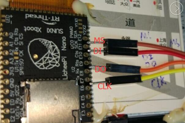
离线
#56 2020-05-15 12:55:12 分享评论
离线
#57 2020-05-15 16:11:52 分享评论
- kq851211
- 会员
- 注册时间: 2020-05-01
- 已发帖子: 49
- 积分: 34.5
Re: step by step 全志 f1c100s MDK 裸奔各种外设(参考N3290x)
我这样搭线不行,必须用转接板?
离线
#58 2020-05-15 16:17:35 分享评论
- kq851211
- 会员
- 注册时间: 2020-05-01
- 已发帖子: 49
- 积分: 34.5
Re: step by step 全志 f1c100s MDK 裸奔各种外设(参考N3290x)
我J-Link Commander 可以连接成功呀。但就是keil调试不了。keil调试要插sd卡吗?我nano板上没焊spi flash。
离线
#59 2020-05-15 16:19:46 分享评论
离线
#60 2020-05-15 16:46:47 分享评论
- kq851211
- 会员
- 注册时间: 2020-05-01
- 已发帖子: 49
- 积分: 34.5
Re: step by step 全志 f1c100s MDK 裸奔各种外设(参考N3290x)
jlink可以检测到,用命令也可以往sram里写数据读数据。但就是keil调试不了,提示那错误。我下的那工程( f1c100s_project_run_in_sram_2.7z)直接就可以调试吗?要不要配置其他什么什么东西?jlink要不要配置什么?
离线
#61 2020-05-15 16:50:20 分享评论
Re: step by step 全志 f1c100s MDK 裸奔各种外设(参考N3290x)
kq851211 wrote:
jlink可以检测到,用命令也可以往sram里写数据读数据。但就是keil调试不了,提示那错误。我下的那工程( f1c100s_project_run_in_sram_2.7z)直接就可以调试吗?要不要配置其他什么什么东西?jlink要不要配置什么?
这个demo不需要另外配置啥,因为sram无需初始化。
截图看下是什么错误?
离线
#62 2020-05-15 16:53:39 分享评论
- kq851211
- 会员
- 注册时间: 2020-05-01
- 已发帖子: 49
- 积分: 34.5
Re: step by step 全志 f1c100s MDK 裸奔各种外设(参考N3290x)
离线
#64 2020-05-15 17:10:05 分享评论
- kq851211
- 会员
- 注册时间: 2020-05-01
- 已发帖子: 49
- 积分: 34.5
Re: step by step 全志 f1c100s MDK 裸奔各种外设(参考N3290x)
恩,可以了,谢谢
离线
#65 2020-05-15 17:11:07 分享评论
- kq851211
- 会员
- 注册时间: 2020-05-01
- 已发帖子: 49
- 积分: 34.5
Re: step by step 全志 f1c100s MDK 裸奔各种外设(参考N3290x)
弱弱的问一下,F1C100S的sram地址怎么是0?我在文档上没找到呀
离线
#66 2020-05-15 17:14:11 分享评论
- kq851211
- 会员
- 注册时间: 2020-05-01
- 已发帖子: 49
- 积分: 34.5
Re: step by step 全志 f1c100s MDK 裸奔各种外设(参考N3290x)
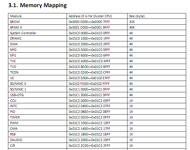
我只在文档上发现这个。不过是 Allwinner_F1C200s处理器用户手册 里的。应该和F1C100s是一样的吧
离线
#67 2020-05-16 13:33:44 分享评论
- kq851211
- 会员
- 注册时间: 2020-05-01
- 已发帖子: 49
- 积分: 34.5
Re: step by step 全志 f1c100s MDK 裸奔各种外设(参考N3290x)
哪位大神能否解释下为什么sram地址是0?文档上0地址不是BROM吗?
离线
#68 2020-05-16 14:19:35 分享评论

Re: step by step 全志 f1c100s MDK 裸奔各种外设(参考N3290x)
kq851211 wrote:
哪位大神能否解释下为什么sram地址是0?文档上0地址不是BROM吗?
全志F1C100s这款芯片是ARM926内核,通过学习其启动流程,可以知道bootloader的原理。可是由于资料的缺少,以至于,我对于它的启动流程,也只是猜测,并未发现有比较严格的描述。因此对于这个芯片的启动流程,任何回答,我认为都不严谨,但是不影响我们对其进行学习和开发。这部分,比较难以描述清楚,只能通过提问-回答的方式来描述。
(1)芯片上电后,做什么事情呢?
F1C100s上电后,芯片内部接通BROM,执行BROM里的程序。
==>BROM里的程序做什么事情呢?
①检查SDIO接口挂接的存储器是否存在有效魔术头。存在,则根据魔术头加载此存储器的程序,并执行。否则执行下一步。
②检查SPI接口挂接的存储器是否存在有效魔术头。存在,则根据魔术头加载此存储器的程序,并执行。否则执行下一步。
③检测不到有有效程序,芯片就进入FEL模式。
==>魔术头是什么呢?
魔术头应该是96字节的一组数据,里面描述了用于SPL相关信息,用于给BROM识别存储器是否存在有效程序。其中包含了,程序的体积,运行地址,等数据。
==>FEL模式是什么呢?
进入FEL模式,我们可以使用软件sunxi-tools通过USB给芯片下载程序到flash等存储器中。
==>芯片如何跳转到用户程序入口呢?
根据本教程对此问题作答,BROM识别到SPI Flash存在有效程序后,会根据魔术头的内容加载SPI Flash里的数据,到芯片的SRAM0中。
注意,这一块SRAM0位于0X00000000地址处,与BROM地址重合,在BROM启动加载代码时,BROM已经失效。也就是说,我们的程序是无法访问BROM的,只能访问BROM失效后的,并且地址与BROM重合的SRAM0。加载完之后,跳转执行。跳转到什么地方执行?不知道,理论上是0X00000000地址,然后执行复位异常的代码。
由于SRAM0的空间有效,非常小,应该只有45KB左右(理论上是32KB,但是经过测试,可以用45KB)。所以,加载进SRAM0的代码需要负责把体积大的程序复制到DRAM里面,然后跳转过去执行。
这个流程描述的非常模糊,可以这样表示:
·BROM里的程序负责加载bootloader到SRAM0,然后跳转执行。
·bootloader程序负责加载APP到DRAM,然后跳转执行。
有可能APP的体积非常大,加载过程很久,所以可以在加载APP之前,显示产品Logo。
最近编辑记录 LinjieGuo (2020-05-16 14:20:16)
离线
#69 2020-05-16 17:32:02 分享评论
- kq851211
- 会员
- 注册时间: 2020-05-01
- 已发帖子: 49
- 积分: 34.5
Re: step by step 全志 f1c100s MDK 裸奔各种外设(参考N3290x)
清楚了,谢谢。
离线
#70 2020-05-16 17:44:27 分享评论
- kq851211
- 会员
- 注册时间: 2020-05-01
- 已发帖子: 49
- 积分: 34.5
Re: step by step 全志 f1c100s MDK 裸奔各种外设(参考N3290x)
请问如果我写了一个程序,要烧到spi flash里运行,是不是必须要在这程序里加魔术头?要怎么加?是用那个mksunxi工具加吗?
离线
#71 2020-05-16 18:07:22 分享评论
离线
#72 2020-05-16 18:17:35 分享评论
- kq851211
- 会员
- 注册时间: 2020-05-01
- 已发帖子: 49
- 积分: 34.5
Re: step by step 全志 f1c100s MDK 裸奔各种外设(参考N3290x)
怎么加魔术头呀?
离线
#74 2020-05-16 18:31:50 分享评论
- kq851211
- 会员
- 注册时间: 2020-05-01
- 已发帖子: 49
- 积分: 34.5
Re: step by step 全志 f1c100s MDK 裸奔各种外设(参考N3290x)
我有mksunxi.exe工具,是不是可以直接用命令 mksunxi.exe xx.bin,就可以生成加好魔术头的xx.bin文件了?
离线
#76 2020-05-26 09:43:59 分享评论
- xsxusen05
- 会员
- 注册时间: 2020-03-08
- 已发帖子: 22
- 积分: 7
Re: step by step 全志 f1c100s MDK 裸奔各种外设(参考N3290x)
能不能把N3290x的数据手册也放上来呢?作为参考好。新唐官网上找不到。
离线
#78 2020-05-27 13:16:46 分享评论
- liuyuedong
- 会员
- 注册时间: 2020-02-09
- 已发帖子: 38
- 积分: 28
Re: step by step 全志 f1c100s MDK 裸奔各种外设(参考N3290x)
感觉f1c100s和新唐的NUC970系列的片子差不多,就是f1c100s资料太少了,新唐的资料还好找到,就是价格比全志的贵多了
离线
#79 2020-06-02 09:13:50 分享评论
- 房地产
- 会员
- 注册时间: 2020-03-02
- 已发帖子: 27
- 积分: 27
Re: step by step 全志 f1c100s MDK 裸奔各种外设(参考N3290x)
这个帖子里的资料真实太全了,好好消化一下
离线
#80 2020-06-23 10:52:29 分享评论
- 2448005461@qq.com
- 会员
- 注册时间: 2020-06-23
- 已发帖子: 3
- 积分: 3
Re: step by step 全志 f1c100s MDK 裸奔各种外设(参考N3290x)
买了一个nano刚到,准备好好学习一下
离线
#81 2020-06-23 14:23:45 分享评论
- zhou_yutao
- 会员
- 注册时间: 2018-10-25
- 已发帖子: 1
- 积分: 1
Re: step by step 全志 f1c100s MDK 裸奔各种外设(参考N3290x)
晕哥:哪儿可以买到带LicheePi Nano Dock底板的开发板?想试试alsa声音.
离线
#82 2020-06-23 14:27:23 分享评论
- cplmaomao0
- 会员
- 注册时间: 2020-06-23
- 已发帖子: 14
- 积分: 99
Re: step by step 全志 f1c100s MDK 裸奔各种外设(参考N3290x)
这个确实牛,淘宝有卖keil开发环境,貌似不错
离线
#83 2020-07-04 15:07:50 分享评论
- billy226
- 会员
- 注册时间: 2020-07-04
- 已发帖子: 3
- 积分: 3
Re: step by step 全志 f1c100s MDK 裸奔各种外设(参考N3290x)
刚入手一块F1C200S,进来跟进学习
离线
#84 2020-07-25 21:34:19 分享评论
- MyCuphead
- 会员
- 注册时间: 2020-07-25
- 已发帖子: 15
- 积分: 0
Re: step by step 全志 f1c100s MDK 裸奔各种外设(参考N3290x)
正在学习,现在借助一个demo,只能用sunxi-fel下载到ram中,keil+jlink还不行,得好好参考下大佬的
离线
#85 2020-07-29 14:54:26 分享评论
- winminwu
- 会员
- 注册时间: 2020-05-06
- 已发帖子: 21
- 积分: 21
Re: step by step 全志 f1c100s MDK 裸奔各种外设(参考N3290x)
kq851211 wrote:
请问如果我写了一个程序,要烧到spi flash里运行,是不是必须要在这程序里加魔术头?要怎么加?是用那个mksunxi工具加吗?
这位兄弟,上面的原理解析的比较详细了,不过关于启动的细节如初始化DDR、时钟等你怎么入手的,可以说说吗
离线
#86 2020-07-29 14:55:49 分享评论
- winminwu
- 会员
- 注册时间: 2020-05-06
- 已发帖子: 21
- 积分: 21
Re: step by step 全志 f1c100s MDK 裸奔各种外设(参考N3290x)
winminwu wrote:
这位兄弟,上面的原理解析的比较详细了,不过关于启动的细节如初始化DDR、时钟等你怎么入手的,可以说说吗
就是那个BootLoader怎么写,然后怎么把指针指向到我的C程序main运行
离线
#87 2020-07-30 20:15:12 分享评论
- demi999
- 会员
- 注册时间: 2020-07-30
- 已发帖子: 11
- 积分: 11
Re: step by step 全志 f1c100s MDK 裸奔各种外设(参考N3290x)
裸跑,那SP应该设置的地址范围是多少?求大佬指点迷津,在这坑上爬了两天了,还是没跳到C的世界。一直卡在SP上,进不去main函数。
大佬们,帮我看下程序哪里有问题,不白看。链接:https://pan.baidu.com/s/14nVgm9-XFiJfsWZ41_N98w
提取码:s4eg
离线
#88 2020-07-31 08:19:15 分享评论
- longxuekai
- 会员
- 注册时间: 2019-11-19
- 已发帖子: 2
- 积分: 2
Re: step by step 全志 f1c100s MDK 裸奔各种外设(参考N3290x)
很强大啊,来学习学习咯,裸跑,喜欢
离线
#89 2020-08-01 10:35:49 分享评论
- winminwu
- 会员
- 注册时间: 2020-05-06
- 已发帖子: 21
- 积分: 21
Re: step by step 全志 f1c100s MDK 裸奔各种外设(参考N3290x)
demi999 wrote:
裸跑,那SP应该设置的地址范围是多少?求大佬指点迷津,在这坑上爬了两天了,还是没跳到C的世界。一直卡在SP上,进不去main函数。
大佬们,帮我看下程序哪里有问题,不白看。链接:https://pan.baidu.com/s/14nVgm9-XFiJfsWZ41_N98w
提取码:s4eg
网站上有点亮LCD的裸机程序,能参考的了吗,还有xboot\src\arch\arm32\mach-f1c100s也有这些启动文件;我参考不了他们这样打包的文件;
你如果调通了,可不可以也分享一下最简单的启动代码都放在同一文件夹下,无关的请不要放,功能就是能像编译xboot那样出来一个bin文件,能用sun-xi命令烧写进spi-flash,最后在main函数点亮一个灯(无关的库函数也不要加哈),不胜感激,小白一个想学习f100s的启动,视频教的都是三星2440、或i.max的[\哭泣]
离线
#90 2020-08-01 10:39:09 分享评论
- winminwu
- 会员
- 注册时间: 2020-05-06
- 已发帖子: 21
- 积分: 21
Re: step by step 全志 f1c100s MDK 裸奔各种外设(参考N3290x)
demi999 wrote:
裸跑,那SP应该设置的地址范围是多少?求大佬指点迷津,在这坑上爬了两天了,还是没跳到C的世界。一直卡在SP上,进不去main函数。
大佬们,帮我看下程序哪里有问题,不白看。链接:https://pan.baidu.com/s/14nVgm9-XFiJfsWZ41_N98w
提取码:s4eg
想以这样的方式,把f100s当单片机用起来;淘宝上买的或这网站下的,keil或Linux下编译的都看不懂它们启动文件,想要个最简单的(不用借助keil)....
离线
#91 2020-11-10 12:06:21 分享评论
- jynjynjyn
- 会员
- 注册时间: 2020-11-10
- 已发帖子: 11
- 积分: 5
Re: step by step 全志 f1c100s MDK 裸奔各种外设(参考N3290x)
哇酷小二 wrote:
kq851211 wrote:
我有mksunxi.exe工具,是不是可以直接用命令 mksunxi.exe xx.bin,就可以生成加好魔术头的xx.bin文件了?
对的.
我在桌面新建一个文件夹把Template.bin文件和mksunxi.exe工具放进去,在命令框CMD中输入 muksunxi.exe Template.bin,提示“加工F1C100s镜像的工具已停止工作”,请问这个是什么问题,怎么解决啊
离线
#92 2020-11-10 13:58:16 分享评论
- redstar
- 会员
- 注册时间: 2020-08-30
- 已发帖子: 2
- 积分: 2
Re: step by step 全志 f1c100s MDK 裸奔各种外设(参考N3290x)
截图看看
离线
#93 2020-11-10 17:34:20 分享评论
- jynjynjyn
- 会员
- 注册时间: 2020-11-10
- 已发帖子: 11
- 积分: 5
Re: step by step 全志 f1c100s MDK 裸奔各种外设(参考N3290x)
redstar wrote:
截图看看
我上传图片一直显示1%不动了。。。。
离线
#94 2020-11-10 18:15:04 分享评论
离线
#95 2021-01-29 11:48:37 分享评论
- yishuizi
- 会员
- 注册时间: 2020-12-15
- 已发帖子: 9
- 积分: 9
Re: step by step 全志 f1c100s MDK 裸奔各种外设(参考N3290x)
论坛有收藏帖子的功能吗,想收藏这个帖子收藏不了
离线
#97 2021-05-26 15:02:09 分享评论
离线
#98 2021-05-29 15:17:19 分享评论
- cube
- 会员
- 注册时间: 2021-03-11
- 已发帖子: 288
- 积分: 202.5
Re: step by step 全志 f1c100s MDK 裸奔各种外设(参考N3290x)
#include <stdio.h>
#include "types.h"
#include "io.h"
#include "reg-ccu.h"

typedef unsigned int u32_t;

#define     __O     volatile
#define     __IO    volatile

#define CPU_PORT_BASE 0x01C20800

#define GPIOG_BASE (CPU_PORT_BASE + 0xD8)
#define GPIOG_INTERRUPT_BASE (GPIO_CPU_INTERRUPT_BASE + 0x20)

typedef struct{
   __IO u32_t CFG[4];
   __IO u32_t DAT;
   __IO u32_t DRV[2];
   __IO u32_t PUL[2];
}GPIO_Typedef;

#define GPIOG ((GPIO_Typedef *)GPIOG_BASE)

static void wait_pll_stable(u32_t base)
{
	u32_t rval = 0;
	u32_t time = 0xfff;

	do {
		rval = read32(base);
		time--;
	} while(time && !(rval & (1 << 28)));
}

static void clock_set_pll_cpu(u32_t clk)
{
	u32_t n, k, m, p;
	u32_t rval = 0;
	u32_t div = 0;

	if(clk > 720000000)
		clk = 720000000;

	if((clk % 24000000) == 0)
	{
		div = clk / 24000000;
		n = div - 1;
		k = 0;
		m = 0;
		p = 0;
	}
	else if((clk % 12000000) == 0)
	{
		m = 1;
		div = clk / 12000000;
		if((div % 3) == 0)
			k = 2;
		else if((div % 4) == 0)
			k = 3;
		else
			k = 1;
		n = (div / (k + 1)) - 1;
		p = 0;
	}
	else
	{
		div = clk / 24000000;
		n = div - 1;
		k = 0;
		m = 0;
		p = 0;
	}

	rval = read32(F1C100S_CCU_BASE + CCU_PLL_CPU_CTRL);
	rval &= ~((0x3 << 16) | (0x1f << 8) | (0x3 << 4) | (0x3 << 0));
	rval |= (1U << 31) | (p << 16) | (n << 8) | (k << 4) | m;
	write32(F1C100S_CCU_BASE + CCU_PLL_CPU_CTRL, rval);
	wait_pll_stable(F1C100S_CCU_BASE + CCU_PLL_CPU_CTRL);
}

void sys_clock_init(void)
{
	write32(F1C100S_CCU_BASE + CCU_PLL_STABLE_TIME0, 0x1ff);
	write32(F1C100S_CCU_BASE + CCU_PLL_STABLE_TIME1, 0x1ff);
	write32(F1C100S_CCU_BASE + CCU_CPU_CFG, 0x00020000);
	write32(F1C100S_CCU_BASE + CCU_AHB_APB_CFG, 0x00012110);

	clock_set_pll_cpu(408000000);
}

void sys_uart_init(void)
{
	u32_t addr;
	u32_t val;

	/* Config GPIOF4 and GPIOF2 to txd0 and rxd0 */
//  addr = 0x01c208b4 + 0x00;//uart0 base
    addr = 0x01c20800 + 0x00;//uart1 base
	val = read32(addr);
	//val &= ~(0xf << ((4 & 0x7) << 2));
	//val |= ((0x3 & 0x7) << ((4 & 0x7) << 2));
    val &= ~((0xf << 8) | (0xf << 12));
    val |= (0x05 << 8) | (0x05 << 12);
	write32(addr, val);

	//val = read32(addr);
	//val &= ~(0xf << ((2 & 0x7) << 2));
	//val |= ((0x3 & 0x7) << ((2 & 0x7) << 2));
	//write32(addr, val);

	addr = 0x01c20068;
	val = read32(addr);
//	val |= 1 << 20; /* Open the clock gate for uart0 */
    val |= 1 << 21; /* Open the clock gate for uart1 */
	write32(addr, val);

	addr = 0x01c202d0;
	val = read32(addr);
//	val |= 1 << 20; /* Deassert uart0 reset */
    val |= 1 << 21; /* Deassert uart1 reset */
	write32(addr, val);

	/* Config uart to 115200-8-1-0 */
//  addr = 0x01c25000; //uart0 base
    addr = 0x01c25400; //uart1 base
	write32(addr + 0x04, 0x0);
	write32(addr + 0x08, 0xf7);
	write32(addr + 0x10, 0x0);
	val = read32(addr + 0x0c);
	val |= (1 << 7);
	write32(addr + 0x0c, val);
	write32(addr + 0x00, 0x37 & 0xff);
	write32(addr + 0x04, (0x37 >> 8) & 0xff);
	val = read32(addr + 0x0c);
	val &= ~(1 << 7);
	write32(addr + 0x0c, val);
	val = read32(addr + 0x0c);
	val &= ~0x1f;
	val |= (0x3 << 0) | (0 << 2) | (0x0 << 3);
	write32(addr + 0x0c, val);
}

void sys_uart_putc(char c)
{
//	u32_t addr = 0x01c25000;//uart0 base
    u32_t addr = 0x01c25400;//uart1 base

	while((read32(addr + 0x7c) & (0x1 << 1)) == 0);
	write32(addr + 0x00, c);
}

int main(void)
{
    sys_clock_init();
    sys_uart_init();

    while(1)
    {
        sys_uart_putc('A');
    }

    return 0;
}
MDK widora r3 裸奔 工程, UART1 (PA2, PA3)输出A:
离线
#99 2021-05-29 16:02:32 分享评论
- cube
- 会员
- 注册时间: 2021-03-11
- 已发帖子: 288
- 积分: 202.5
Re: step by step 全志 f1c100s MDK 裸奔各种外设(参考N3290x)
MDK + GNU GCC 版本: widora_r3_uart1_pa2_pa3_gnu_20210529.zip
离线
#100 2021-05-31 15:40:29 分享评论
- ueiia
- 会员
- 注册时间: 2021-04-30
- 已发帖子: 30
- 积分: 8
Re: step by step 全志 f1c100s MDK 裸奔各种外设(参考N3290x)
新人入坑,有个问题一直想问
我现在spl+RTT.bin已经可以运行起来了,我想用jlink调试RTT.bin,大神给的都是在SRAM里面调试,我的RTT.bin是在DDR里面的,用eclipse调试时候就会复位芯片,导致DDR也复位了,程序没办法载入到DDR里面,不知道各位大神有没有相应的解决方案可以参考一下
离线
#101 2021-05-31 17:16:37 分享评论
#102 2021-06-24 16:36:34 分享评论
- szchen2006
- 会员
- 注册时间: 2019-10-09
- 已发帖子: 216
- 积分: 166.5
Re: step by step 全志 f1c100s MDK 裸奔各种外设(参考N3290x)
离线
- 不通过:与技术无关
#103 2021-08-04 15:16:35 分享评论
- 疆海
- 会员
- 注册时间: 2021-08-04
- 已发帖子: 2
- 积分: 1
Re: step by step 全志 f1c100s MDK 裸奔各种外设(参考N3290x)
终于看完了该帖子,不错,学习,感谢大神些,突然发现这个网址后,比追剧舒服多了
离线
#104 2021-09-02 09:34:38 分享评论
- abbottn
- 会员
- 注册时间: 2020-07-16
- 已发帖子: 6
- 积分: 2.5
Re: step by step 全志 f1c100s MDK 裸奔各种外设(参考N3290x)
想下载还挺不容易,分好高
离线
#105 2021-09-19 15:32:38 分享评论
- lg676041036
- 会员
- 注册时间: 2021-07-09
- 已发帖子: 39
- 积分: 28
Re: step by step 全志 f1c100s MDK 裸奔各种外设(参考N3290x)
终于找到MDK的调试了
离线
#106 2021-10-25 15:47:35 分享评论
- chenpeng30
- 会员
- 注册时间: 2021-10-25
- 已发帖子: 7
- 积分: 7
Re: step by step 全志 f1c100s MDK 裸奔各种外设(参考N3290x)
各位大佬, 怎么赚取积分, 下载不了!~
离线
#109 2021-12-18 10:36:16 分享评论
- bailangcn
- 会员
- 注册时间: 2021-09-24
- 已发帖子: 15
- 积分: 10
Re: step by step 全志 f1c100s MDK 裸奔各种外设(参考N3290x)
离线
- 不通过:其他
#110 2022-03-29 17:27:54 分享评论
- 超级网吧
- 会员
- 注册时间: 2022-03-29
- 已发帖子: 5
- 积分: 0
Re: step by step 全志 f1c100s MDK 裸奔各种外设(参考N3290x)
一直用单片机,想试试f1c200s当单片机用,追随至此,顶礼膜拜:)
离线
#111 2022-04-21 17:53:25 分享评论
- bigbat
- 会员
- 注册时间: 2022-01-30
- 已发帖子: 71
- 积分: 21
Re: step by step 全志 f1c100s MDK 裸奔各种外设(参考N3290x)
我的板子没有调试口,看来有困难
离线
#112 2022-04-22 00:08:25 分享评论
- happy粥
- 会员
- 注册时间: 2022-04-12
- 已发帖子: 8
- 积分: 18
Re: step by step 全志 f1c100s MDK 裸奔各种外设(参考N3290x)
离线
- 不通过:与技术无关
#113 2022-04-27 16:34:08 分享评论
- LwPerson
- 会员
- 注册时间: 2022-04-27
- 已发帖子: 3
- 积分: 23
Re: step by step 全志 f1c100s MDK 裸奔各种外设(参考N3290x)
@LinjieGuo 用MDK编译了一个F1C200S的裸机的串口+点灯程序,用sunxi-fel.exe通过fel模式把代码加载到0x0000地址开始的空间并运行,串口可以正常输出打印数据,LED也可以正常闪烁。 发现0x0000开始的32KB的BROM地址正常可读写, 0x10000开始的40KB的SRAM A地址无论写入什么数据读出的数据都是0
离线
#114 2022-04-29 17:04:39 分享评论
- jxlxh
- 会员
- 注册时间: 2022-03-27
- 已发帖子: 9
- 积分: 9
Re: step by step 全志 f1c100s MDK 裸奔各种外设(参考N3290x)
@晕哥
timer0中断问题
//void _mOldIrqVect = (void volatile *)0x38;
(void volatile )0x38 = (void volatile)sysIrqHandler;
这个何解?是作为中断矢量0x38吗?
我程序在SDRAM中运行,不能进中断,一运行PC就停在0x00000004处
离线
#116 2022-09-14 10:13:54 分享评论
- mind
- 会员
- 注册时间: 2022-08-16
- 已发帖子: 6
- 积分: 1
Re: step by step 全志 f1c100s MDK 裸奔各种外设(参考N3290x)
裸奔 DVP CSI的,有没有调通的,linux主线的启动时间剪裁后还是太长,客户不接受
离线
#117 2022-10-20 17:17:49 分享评论
- 右半边天天晴
- 会员
- 注册时间: 2022-10-18
- 已发帖子: 4
- 积分: 4
Re: step by step 全志 f1c100s MDK 裸奔各种外设(参考N3290x)
大佬们,我写了一个最简单的点灯程序,用mksunxi.exe工具将这个点灯程序打包后,通过sunxi-fel和dfu-util工具下载到128MiB的SPI Nand flash中,可是下载完成后重新上电,电脑设备管理器上还是会显示fel设备,不知道为什么板子还是会进入fel模式,是因为我这个点灯程序通过mksunxi工具打包的魔术头有问题造成的吗?是不是只要魔术头没有问题,不管魔术头后面跟的程序是啥都可以被BROM认为这段代码是有效的,然后将32KiB代码加载到内部的sram上运行呢?有清楚地大佬还望指教指教,万分感谢。
离线
#118 2022-11-25 00:09:43 分享评论
- Simn
- 会员
- 注册时间: 2021-12-16
- 已发帖子: 33
- 积分: 3
Re: step by step 全志 f1c100s MDK 裸奔各种外设(参考N3290x)
J-link适配器原件还是复印件? 哪个版本? 我在哪里可以买到?
离线
#120 2023-04-28 10:07:46 分享评论
- 家猫戏很足
- 会员
- 注册时间: 2018-09-16
- 已发帖子: 14
- 积分: 4
Re: step by step 全志 f1c100s MDK 裸奔各种外设(参考N3290x)
提示:*** Error: Failed to execute 'arm-none-eabi-gcc'
arm-none-eabi-gcc已经安装配置到环境变量里了,是什么原因呢?
离线
#121 2023-04-28 13:53:56 分享评论
- 家猫戏很足
- 会员
- 注册时间: 2018-09-16
- 已发帖子: 14
- 积分: 4
Re: step by step 全志 f1c100s MDK 裸奔各种外设(参考N3290x)
家猫戏很足 wrote:
提示:*** Error: Failed to execute 'arm-none-eabi-gcc'
arm-none-eabi-gcc已经安装配置到环境变量里了,是什么原因呢?
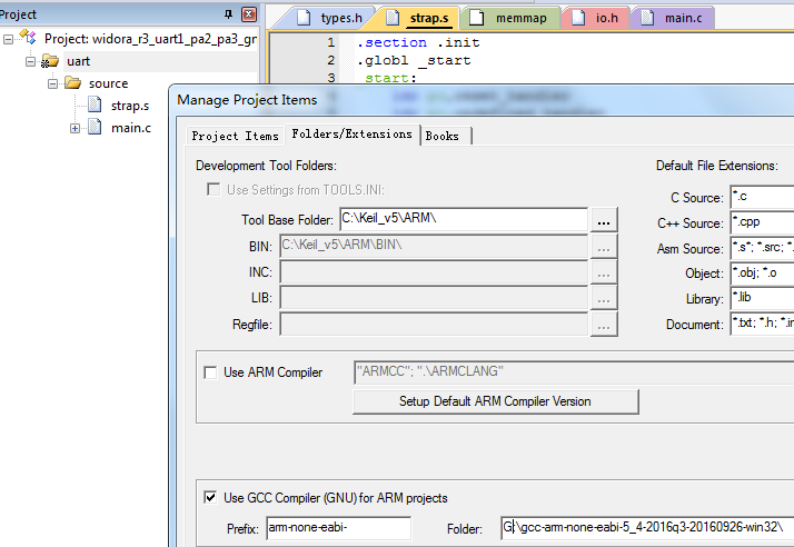
查到原因了,右击项目--Manage Project Items--Floders/Externsion--Folder 工程是gcc-arm绝对地址,工程里带了Toolchain
但是还有一个问题,用新版的gcc-arm会报 multiple definition 错误,对gcc-arm不太熟悉,怎么解决呢
离线
#122 2023-09-01 01:42:47 分享评论
- Lunasama
- 会员
- 注册时间: 2023-01-10
- 已发帖子: 14
- 积分: 24
Re: step by step 全志 f1c100s MDK 裸奔各种外设(参考N3290x)
@晕哥 TIM0的中断源不是0x0034吗,怎么程序写的是0x38
离线
#123 2023-09-01 23:12:30 分享评论
- Lunasama
- 会员
- 注册时间: 2023-01-10
- 已发帖子: 14
- 积分: 24
Re: step by step 全志 f1c100s MDK 裸奔各种外设(参考N3290x)
Lunasama wrote:
@晕哥 TIM0的中断源不是0x0034吗,怎么程序写的是0x38
找了一下问题,我之所以在0x34能进IRQ是因为我在写SPL的时候瞎折腾搞出的问题:P
离线
#124 2023-09-10 12:04:04 分享评论
- vigour1000
- 会员
- 注册时间: 2018-11-19
- 已发帖子: 103
- 积分: 4
Re: step by step 全志 f1c100s MDK 裸奔各种外设(参考N3290x)
LCD能显示常吗,这边只有背光
离线
#128 2024-03-12 17:25:10 分享评论
- stone
- 会员
- 注册时间: 2024-03-12
- 已发帖子: 6
- 积分: 2
Re: step by step 全志 f1c100s MDK 裸奔各种外设(参考N3290x)
这个芯片我用sunxi-fel来读或者写,总是会半路出错,也不知道怎么回事
离线
#129 2024-03-28 14:21:39 分享评论
- _XJ_
- 会员
- 注册时间: 2024-03-12
- 已发帖子: 8
- 积分: 1
Re: step by step 全志 f1c100s MDK 裸奔各种外设(参考N3290x)
我调试到某个地方就会提示“Cannot read memory”是什么原因
离线
#131 2024-09-18 10:46:21 分享评论
- cris8259
- 会员
- 注册时间: 2019-09-25
- 已发帖子: 283
- 积分: 82
Re: step by step 全志 f1c100s MDK 裸奔各种外设(参考N3290x)
mdk 启动调试 提示 Error: Target DLL has been cancelled. Debugger aborted ! 是什么原因
离线
东莞哇酷科技有限公司开发